3D Printed Ion Trap
Lead inventor: David Allcock
Co-inventors: Morgan Brown, Tim Gardner, Alexander Quinn
Licensing contact: Christine Gramer
1. Technology Overview
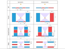
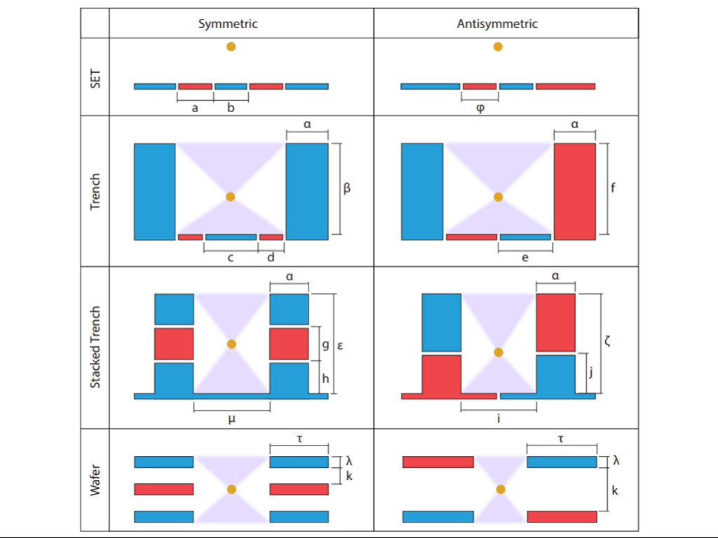
The invention introduces a 3D-printed ion trap designed for quantum computing applications. This innovative device leverages additive 3D printing of glass structures to create ion traps that can be integrated onto wafers containing micro-fabricated elements. The technology offers significant potential for improving trapping efficiency, depth, and harmonicity compared to traditional 2D surface-electrode traps. Currently in the development stage, this technology holds strong potential for commercialization in quantum computing, semiconductor manufacturing, and related fields.
2. Key Features and Benefits
- Additive manufacturing: Simplifies fabrication and allows integration with micro-fabricated components.
- Enhanced trapping properties: Improved efficiency, depth, and harmonicity compared to 2D traps.
- Scalability: Established 3D printing techniques enable large-scale production.
- Versatility: Applicable to a wide range of quantum computing and advanced manufacturing applications.
- Integration: Compatible with existing micro-fabrication processes and semiconductor technologies.
3. Applications and Market Focus
- Quantum computing: Enhancing the performance and scalability of quantum computing systems.
- Semiconductor manufacturing: Providing advanced fabrication methods for semiconductor devices.
- MEMS: Supporting the development of micro-electromechanical systems with improved properties.
- Photonics and optoelectronics: Enabling advanced applications in photonics and optoelectronics.
- Research and development: Facilitating further innovation in quantum computing and advanced manufacturing technologies.
4. Commercial Advantages
- Strategic benefits: Offers a scalable and efficient solution for ion trap fabrication in quantum computing.
- Implementation advantages: Simplifies the development of high-performance ion traps and related devices.
- Market positioning: Positions the technology as a key enabler in quantum computing and advanced manufacturing sectors.
- Competitive edge: Provides a unique and effective method for improving trapping properties and fabrication efficiency.
5. Partnership Opportunities
- Licensing partners: Ideal for companies in quantum computing, semiconductor manufacturing, and MEMS.
- Cross-sector benefits: Offers advantages to multiple industries, including photonics and optoelectronics.
- Market opportunities: Addresses diverse market needs, from quantum computing to advanced manufacturing.
- Collaborative development: Potential for joint ventures with research institutions and technology firms to further enhance the technology.
Patent filing: WO2023219863A1
Image Gallery